cadence circuit design
OrCAD PCB Designer file extensions. 9 Pics about OrCAD PCB Designer file extensions : cadence tutorial : Operational amplifier design in cadence Part 1b, what is physical design - VLSI- Physical Design For Freshers and also Cadence tutorial - Layout of CMOS NOR gate - YouTube.
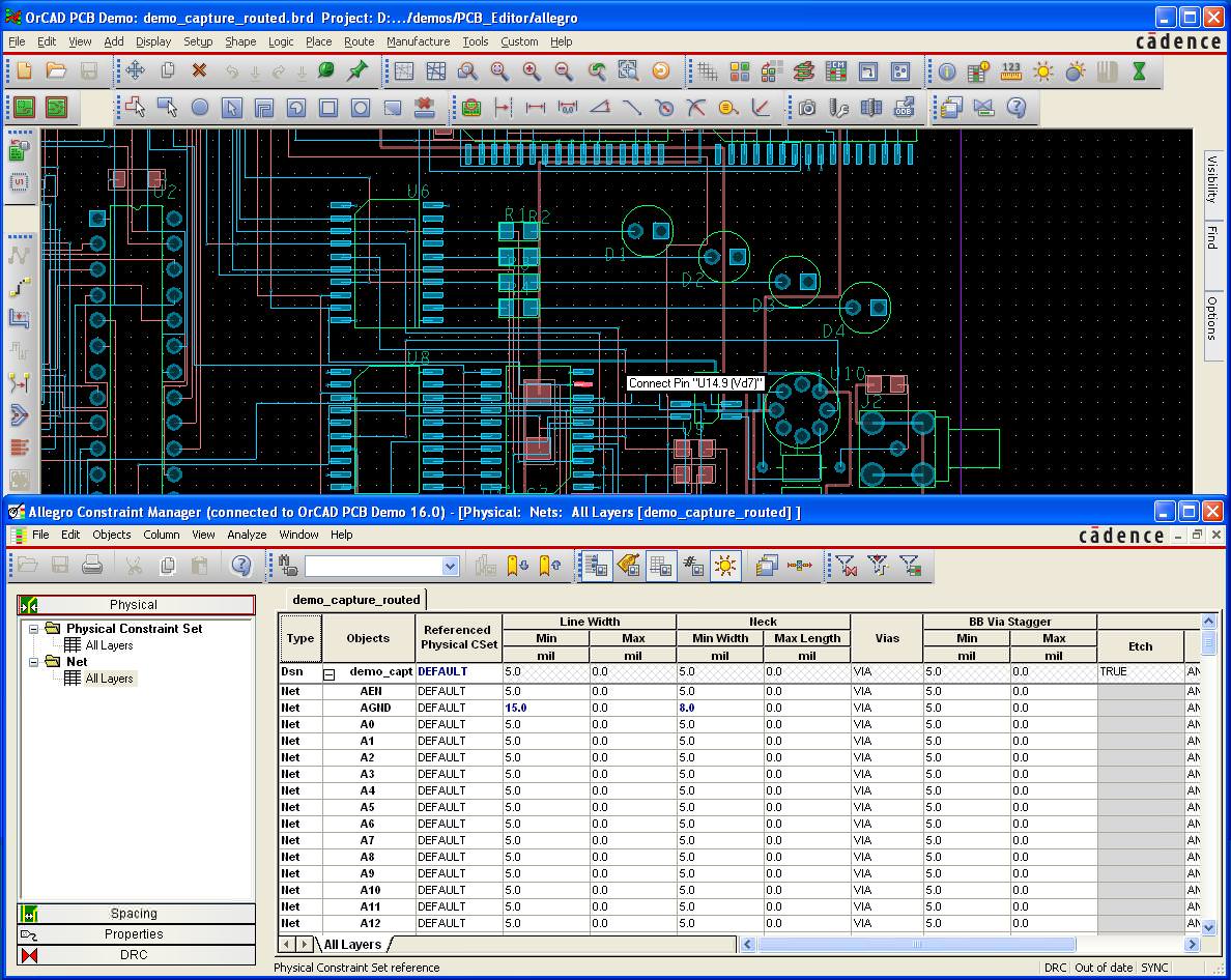
OrCAD PCB Designer File Extensions
 www.file-extensions.org
orcad pcb designer file extensions
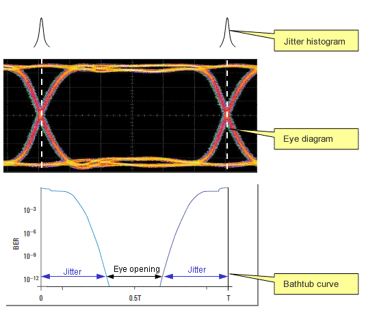
Low Jitter Saw OSC | Circuit Design | IC Partners Info. | Epson Crystal
 www5.epsondevice.com
ber jitter saw rate error bit oscillator ic partners notes user low www5 epsondevice
Cadence Tutorial - Layout Of CMOS NOR Gate - YouTube
 www.youtube.com
layout cadence gate nor cmos tutorial
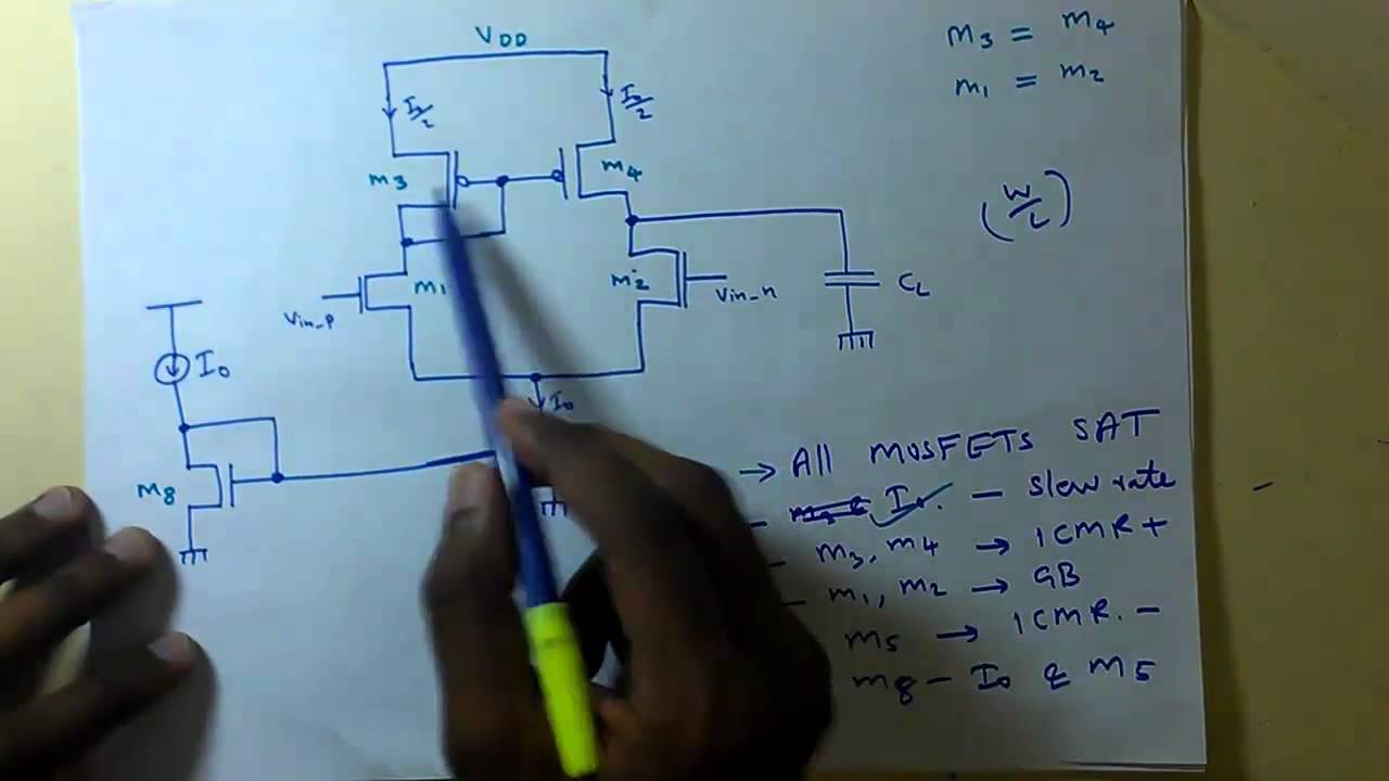
Cadence Tutorial : Operational Amplifier Design In Cadence Part 1b
 www.youtube.com
amplifier cadence amp operational tutorial
HB And TRANSIENT Shows Different Result Regarding Dc Block - RF Design
 community.cadence.com
cadence hb regarding transient result block dc shows different community thanks
Voltage Controlled Oscillators | PSpice
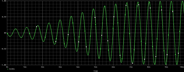 www.pspice.com
simulation controlled voltage vco oscillators pspice results figure fig3
Catching Layout-dependent Effects On-the-fly - Tech Design Forum Techniques
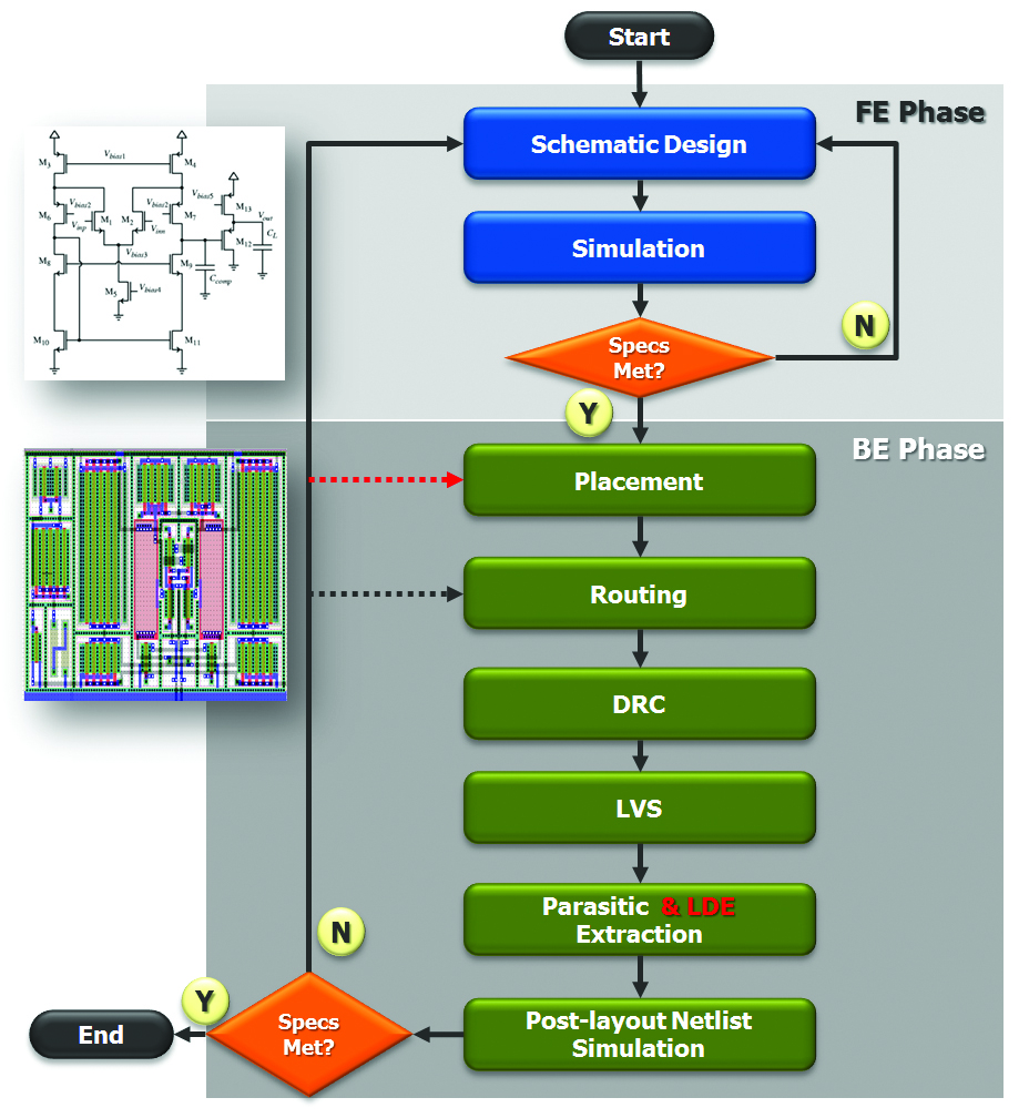 www.techdesignforums.com
flow ic layout custom dependent fly simulation effects typical catching figure techdesignforums lde practice
PCB Design Software – Which One Is Best?
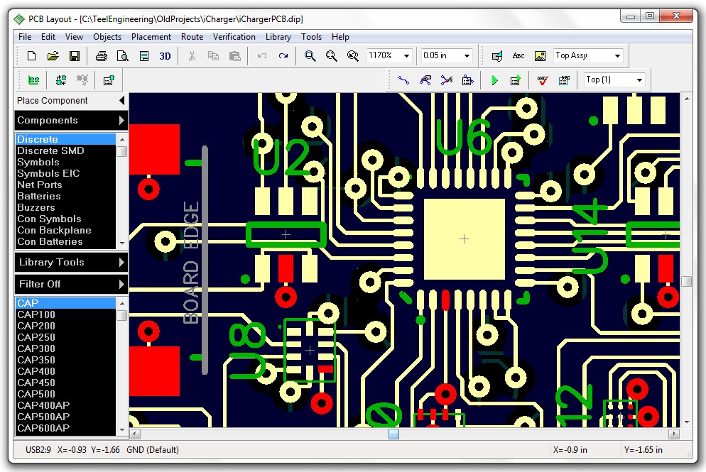 predictabledesigns.com
pcb cad software component electrical engineering layout reverse diptrace module which 3d eagle creation programs symbol drawing
What Is Physical Design - VLSI- Physical Design For Freshers
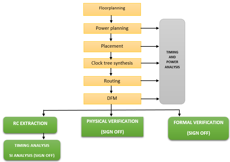 www.physicaldesign4u.com
vlsi
Layout cadence gate nor cmos tutorial. Pcb cad software component electrical engineering layout reverse diptrace module which 3d eagle creation programs symbol drawing. Cadence hb regarding transient result block dc shows different community thanks